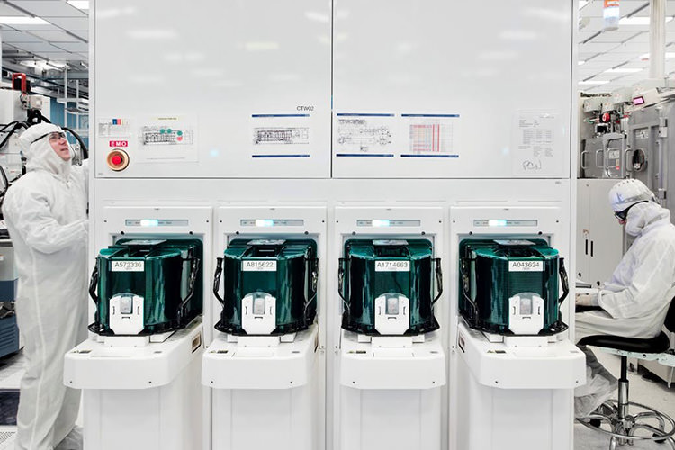
IBM’s 5nm technology fits 30 billion transistors on a fingerprint chip
IBM has announced the production of 5-nanometer chips based on a new standard that will say goodbye to the FinFET standard. The process uses a new structure with a stack of four nanoplates to fit 30 billion transistors on a chip the size of a knuckle. This means that extremely powerful chips will be produced in very small dimensions in terms of processing. Minimizing lithography always means higher productivity and lower power consumption in the same architecture, and with IBM’s new technology, it is possible to keep power consumption low by increasing processing power.
Moore’s Law, which was first proposed in the 1970s, stated that the number of transistors on a chip would double every two years. But in recent years, this law has been challenged by the physical limitations of silicon, slowing the rate of transistor additions. Currently, 14-nanometer chips are widely used in the consumer electronics market. However, Intel and Samsung have switched to 10-nanometer chips to stay ahead of their competitors.
Interestingly, IBM unveiled a 7nm experimental chip in 2015 in collaboration with Samsung and GlobalFoundries that could fit 20 billion transistors on a single die. They believe that 7nm chips could be commercially available in 2019.
Interestingly, IBM unveiled a 7nm experimental chip in 2015 in collaboration with Samsung and GlobalFoundries that could fit 20 billion transistors on a single die. They believe that 7nm chips could be commercially available in 2019.
That’s why IBM’s 5nm chip uses nano-silicon planes that can send signals through four gates at once, compared to three in FinFET. IBM engineers used extreme ultraviolet (EUV) lithography, a process that uses much higher wavelengths of light energy to etch patterns onto the chip’s silicon wafer. This allows for much more detail on the chip, and unlike current lithography processes, the chip’s power and efficiency can be controlled.
If we compare IBM’s 5nm lithography with the current 10nm ones, the new lithography can increase efficiency by 40% at the same energy, and if we want to get the same efficiency from both lithographies, the energy consumption in 5nm lithography is reduced by 75%, which is a significant amount.
However, since 10nm lithography has only recently been used and 7nm lithography is set to be used in 2019, it is expected that chips based on 5nm lithography will be released in the next 4 or 5 years.


Leave a Reply
Want to join the discussion?Feel free to contribute!